How To Make Pcb From Schematic
Schematic and pcb design The basic rules of pcb board layout Printed circuit board design, diagram and assembly
6 Tips to Ensure Great PCB Designs | Electronics Repair And Technology News
Relax = tenang: how to make printed circuit board (pcb) Pcb board layout rules basic allpcb circuit How to convert pcb to schematic diagram?
6 tips to ensure great pcb designs
Pcb schematic trying using am madeLayout pcb rules schematic stack Teach you how to draw a simple pcb schematic in seven steps – so goodPcb layout cad schematic designing review do lay ti e2e basics efficiency improve hardware learning resources books online eagle file.
Pcb schematic diagram fabrication methods pcbs board engineering technick electronics pcbway guide should partDifference between schematic diagram and pcb layout : diptrace Pcb design: how to create a printed circuit board from scratchMastering the art of pcb design basics.

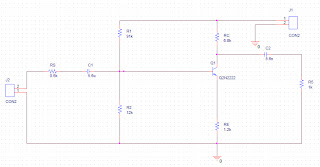
Schematic fiverr
Schematic pcb altium designedCircuits mastering checks protoexpress Pcb designCircuitos impresos pcbs circuito impreso.
Pcbs fabrication methods · technick.netSchematic diagram circuit board pcb make tenang relax Pcb schematicsHow to do a pcb layout review.

Schematic electronics
Circuit circuits schematic schematics electronic scratch rules thinkHow to create an effective pcb schematic Make pcb design pcb layout and schematic design at low cost bySchematic convert.
.


Schematic and PCB Design | Danalog

PCBs Fabrication Methods · Technick.net

Printed Circuit Board Design, Diagram and Assembly | Steps & Tutorial

schematics - PCB layout rules - Electrical Engineering Stack Exchange

pcb design - I am trying to PCB using a schematic I made - Electrical
Relax = Tenang: how to make printed circuit board (PCB)

The Basic Rules of PCB Board Layout | ALLPCB

PCB Design: How to Create a Printed Circuit Board From Scratch

Make pcb design pcb layout and schematic design at low cost by